
7. Integrated circuits
Integrated Circuits play a very important part in electronics. Most are specially made for a specific task and contain up to thousands of transistors, diodes and resistors. Special purposes IC's such as audio-amplifiers, FM radios, logic blocks, regulators and even a whole micro computers in the form of a micro controller can be fitted inside a tiny package. Some of the simple Integrated Circuits are shown in figure 7.1.

Fig. 7.1: Integrated circuits
Depending on the way they are manufactured, integrated circuits can be divided into two groups: hybrid and monolithic. Hybrid circuits have been around longer. If a transistor is opened, the crystal inside is very small. This means a transistor doesn't take up very much space and many of them can be fitted into a single Integrated Circuit.
The pin-out for some of the common packages is shown in Figure 7.2:
The pin-out for some of the common packages is shown in Figure 7.2:

Fig. 7.2: Pin-out and symbols for some common integrated circuits
Most integrated Circuits are in a DIL package - Dual In Line, meaning there are two rows of pins. (DIL16 and DIL8 are shown in 7.2b and 7.2c). The device is viewed from the top and the pins are numbered in an anti-clockwise direction.
High power integrated circuits can generate a lot of heat and they have a metal tag that can be connected to a heatsink to dissipate the heat. Examples of these IC's are shown in 7.2d and 7.2e, and 7.2f.
Symbols used to represent integrated circuits are shown in 7.2g and 7.2i. Symbol 7.2g is commonly used to represent amplifiers.
Figure 7.2i shows an operational amplifier. Signs + and - represent inverting and non-inverting inputs. The signal to be amplified is applied between one of the inputs and ground (ground and supply aren't represented, but are necessary for the circuit to operate).
Integrated circuits can be divided into two further groups: analog (linear) and digital. The output voltage of a linear circuits is continuous, and follows changes in the input. Typical representative of a linear IC is an integrated audio amplifier. When a signal from a microphone is connected to the input the output will vary in the same way as the voltage from the microphone. If watched on an oscilloscope, the signal on the output will be the same shape as the mic's signal, only the voltage will be higher depending on the amplification of the integrated circuit.
It is a different situation with digital IC's. Their output voltage is not continuous. It is either LOW or HIGH and it changes from one state to the other very quickly.
7.1 Analog integrated circuits
While on the topic of analog circuits, we will look at the LM386 IC. It has all the components for a complete audio-amplifier. Figure 7.3a shows an example of an amplifier made with this integrated circuit, which can be used as a complete amplifier for a walkman, interphone, cassette player or some other audio device. It can also be used as a test circuit for troubleshooting.

Fig. 7.3: a - A low frequency amplifier using the LM386
The signal is brought to the non-inverting input (between pin 3 and ground). Inverting input (pin 2) is connected to ground. If 10µF is placed between pins 1 and 8 a voltage amplification of 200 is created. If this capacitor is removed the amplification is 20. It is possible to achieve in-between amplification by adding a resistor and connecting it in series with the capacitor.
One of the essential components in this circuit is the 100nF capacitor which is placed between pin 6 (which is connected to the positive of the supply) and ground. The capacitor should be ceramic and should be mounted as close to the integrated circuit as possible. This is common practice when working with integrated circuits, even when it isn't shown in the diagram as a capacitor connected between the positive and negative stabilizes the voltage and protects the circuit from spikes and a phenomenon called instability. This is due to inductance in the power supply tracks allowing high currents taken by the IC to upset its operation.
One of the essential components in this circuit is the 100nF capacitor which is placed between pin 6 (which is connected to the positive of the supply) and ground. The capacitor should be ceramic and should be mounted as close to the integrated circuit as possible. This is common practice when working with integrated circuits, even when it isn't shown in the diagram as a capacitor connected between the positive and negative stabilizes the voltage and protects the circuit from spikes and a phenomenon called instability. This is due to inductance in the power supply tracks allowing high currents taken by the IC to upset its operation.
7.2 Digital integrated circuits
The CD4011 will be our "show-and-tell" IC to cover the main characteristics of digital circuits. It is a 14 pin DIL package. The pin-out is shown in figure 7.4a. Note the small half-round slit on one end of the IC. It identifies pin 1. Pins 7 and 14 connect to a supply (battery or DC power supply). Negative is connected to pin 7. Positive is connected to pin 14.
There are four logic NAND gates in a CD4011 IC. Each has two inputs and one output. For gate N1 the inputs are pins 1 and 2, and output is pin 3. The symbol for a NAND gate is displayed in figure 7.4b. The inputs are marked A and B and output is F. The supply voltage can be up to 16v and as low as 5V. The output will deliver up to 10mA at 12v but this is reduced as the supply voltage is reduced.
Figure 7.4b shows the truth table for a NAND gate. It shows the output voltage (voltage between F and ground) with different input states. Because there are only two voltages for every pin, we call them states, with logic zero when the voltage is zero, and logic one when the voltage on the pin is the same as the supply voltage.
From this we can read the second row of the truth table: if logic zero is on both input pins, output is logic one, third row is similar: if the first input is one, and the second one is zero, output is logic one, fourth row: if the first input is zero, and the second one is one, output is logic one. Fifth row is different, since both of its inputs are one, the definition of NAND gate states that the output is zero.

Fig. 7.4: a - 4011 pin placements, b - symbol and the truth table for NAND gates,
Logic circuits have many applications, but their main use is in computer circuits.
The following circuit is a simple example to show how the gates can be connected to produce a project that turns on a globe when a finger is placed on a "touch pad."
The globe turns off after a period of time, determined by the value of the 470u and 2M2 resistor.
The following circuit is a simple example to show how the gates can be connected to produce a project that turns on a globe when a finger is placed on a "touch pad."
The globe turns off after a period of time, determined by the value of the 470u and 2M2 resistor.

The operation of a NAND gate
Lets look at the functionalities of the following circuit. Both inputs of NI1 are connected to each other, so when input P is HIGH, output is zero. This logic zero is passed on to NI2, so no matter what is on the input 6, output 4 is logic one. This means that, between the ground and pin 4, the voltage is equal to 12V.

Fig. 7.5: Sensor switch using a 4011
Current flows through capacitor C and resistor R, so capacitor begins to charge. Every uncharged capacitor behaves like a short circuit. Because of that, when 12V appears on pin 4, it is also present on resistor R and also on pins 8 and 9. Pin 10 shows logic zero because of this which is connected to pin 6. From now on, logic zero on pin 5 is no longer needed because only one input needs to be zero for the output to be logic one. So input P is no longer needed. Gates NI2 and NI3 maintain logic zero on pin 4. How long will this last? It depends on the value of the capacitor and resistor. As the capacitor charges, the voltage on the resistor drops and when it falls to 1/2 of the supply voltage (6V in our case), NI3 detects a low on its inputs so logic one appears on pin 10. Since logic one is now on input 5 (no logic one present on P), and on input 6, output 4 is zero, capacitor dumps its charge via diodes on the inputs on pins 8 and 9 and the circuit starts operating again.
As we saw, for a certain period of time, which is equal to T=0.7*RC output of pin 10 was logic zero. During that time output E (pin 11) is logic one. For example, if R = 2M2 and C=47µF, for time T = 2.2*10^6*47*10^-6 = 94 sec from the moment impulse on input P subsided, voltage on output E is 12V.
The end result of our experiment is on diagram 7.5a. Short positive pulses appearing on P in the time t1 caused a longer variable ulse on output E.
Schematic 7.5b displays this circuit which allows us to light a bulb using four NAND gates interconnected in the way shown on picture 7.5a.
The sensor is two copper (or some other conducting material) plates glued to some non-conducting material (plastics, wood, etc.) in close proximity to each other. So, when we touch the sensor with the tip of our finger, we close the circuit. 12V appears on input P, which in turn conducts the voltage to the output E, resistor R = 22k conducts base current and the bulb lights. When we remove our finger, output E will last for 94 seconds, after which it goes to logic zero and the light goes out.
Transistor T is selected so that its maximum allowed collector current is higher than the current of the globe.
(The globes current flow value is found by dividing its power by its voltage. For example, if its power is P = 6W and voltage is U = 12V, current through the globe is I = P/U = 6W/12V = 0.5A or higher. One thing you must remember with a globe is the starting or "turn-on" current. It is about six times the operating current and the transistor must be able to pass this current for the globe to illuminate.
7.3 Practical examples
Diagram 7.6 shows a circuit for a stereo audio-amp using a TDA4935 IC. It is a modern integrated circuit with two separate pre-amps and stereo outputs.
Left and right input signals are marked UL and UD, which are brought to two inputs of the amplifier. The chip also has built-in heat and overload protection. Maximum output for each amplifier is 15W, so they can be used in stereo mode of 2x15W amplifiers.
Left and right input signals are marked UL and UD, which are brought to two inputs of the amplifier. The chip also has built-in heat and overload protection. Maximum output for each amplifier is 15W, so they can be used in stereo mode of 2x15W amplifiers.

Fig. 7.6: Stereo audio-amplifier using the TDA4935
Another example is an audio amplifier using an LM386 circuit, with a preamp using a BC107 transistor. The series connected capacitor and resistor between pins 1 and 5 produces low frequency amplification (around 100Hz) improving the characteristics of the circuit. This amplifier could be used with any low frequency source (gramophone, microphone, etc.).

Fig. 7.7: complete audio-amplifier using the LM386
The third example is a simple alarm, shown in figure 7.8. It uses a CD4011 IC. Gates NI3 and NI4 form a 600Hz audio oscillator. This signal is amplified using an NPN transistor and passed to an 8R speaker. To hear the 600Hz tone, remove the connection to pin 8 and connect pin 8 to pin 9. This produces a constant tone. Gates NI1 and NI2 form a 4Hz oscillator, whose output is connected to pin 8. This turns the 600Hz tone on and off at 4Hz. To use this alarm in your home, on doors for example, connected pin 1 to 7 via a switch.

Fig. 7.8: Alarm using a CD4011 IC
The last circuit in this chapter is an example of a mono FM receiver using a TDA7088T IC, which can be, along with the SMD components, housed in a match-box along with two miniature watch batteries. You can purchase a ready-built scanning radio in a "junk shop" for as little as $5.00 with stereo head-phones Always look in the toy sections of large stores for the latest technology at the cheapest price.
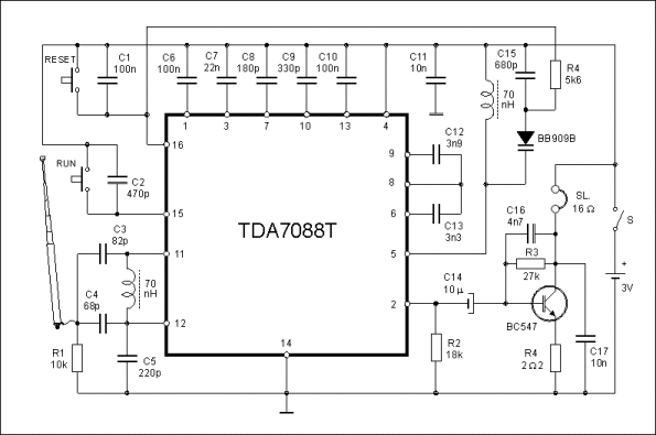
Fig. 7.9: Mono FM radio receiver with an electronic preset
Web site
tags: Integrated Circuits, transistors, diode, resistors
|
|


0 comments:
Post a Comment