When connecting a
solar panel to a
rechargeable battery, it is usually necessary to use a
charge controller circuit to prevent the battery from overcharging.
Charge control can be performed with a number of different circuit types.
Lower power solar systems can use a series analog charge controller. Series regulators control the charging current by interrupting the flow of current from the solar panel to the battery when the battery reaches a preset full voltage. MPPT controllers use an inductor for energy storage and a high frequency switching circuit to transfer the energy to the battery.
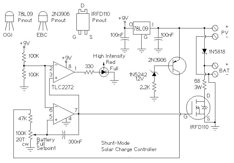
This circuit is for a shunt-mode charge controller. In a shunt-mode circuit, the solar panel is permanently connected to the battery via a series diode. When the solar panel charges the battery up to the desired full voltage, the shunt circuit connects a resistive load across the battery to absorb the excess power from the solar panel. The main advantage of shunt-mode solar regulation is the lack of a switching transistor in the power path between the solar panel and battery. Switching transistors are non-perfect devices, they waste a percentage of available solar power as heat. Inefficiency in the shunt-mode controller’s switching transistor does not effect charging efficiency, it only turns on when excess power is purposely being wasted.

Solar power is routed from the PV panel through the 1N5818 Schottky diode to the battery. When the battery reaches the full setpoint, the output on the lower half of the TLC2272 dual op-amp turns on. This activates the IRFD110 MOSFET transistor and connects the 68 ohm 3W load resistor to the battery. The load across the battery causes the battery voltage to drop, and the comparator circuit turns back off. This oscillation continues while solar power is available. The 300nF capacitor across the op-amp slows the oscillation frequency down to a few hertz. The two 100K resistors in series provide a regulated 4.5V reference point for use as comparator reference points.
The 2N3906 transistor is wired with a zener diode in its base circuit, when the PV voltage is above 12V, the 2N3906 transistor turns on and enables the comparator circuit. The upper half of the TLC2272 op-amp inverts the dump load control signal, this is used to power the high intensity red LED. The LED turns on when the battery reaches the full setpoint. The LED does not waste any useful charging power since it only turns on when the battery is full.
The 78L09 IC provides 9V regulated power to the comparator circuitry. Operational power for this circuit is provided entirely from the PV panel, there is virtually no power taken from the battery at night.
This circuit can be modified for higher amperage by replacing the 1N5818 diode, 68 ohm load resistor and IRFD110 MOSFET with higher power components. If the load resistor is connected directly across the PV panel at noon on a sunny day, the PV output voltage should drop to 12V or less. Higher power PV panels will require a resistor with lower ohms and a higher wattage rating. In cold climates, it may be useful to use the load resistor’s heat to keep the battery warm.
Operation of a high power version of this circuit with a wind generator should be possible, although the author has not tried this. For a 20 amp version of this circuit, the IRFD110 MOSFET should be replaced with an IRFZ44N and the 1N5818 schottky diode should be replaced with a 20L15T. Both of these parts should have large heat sinks. The 68 ohm/3W resistor should be changed to a much larger resistor, An 0.6 ohm/250W resistor would be able to handle 20 amps at 12V.
source : www.solorb.com
tags: solar panel, solar and system