Showing posts with label Timer. Show all posts

Sunday, February 19, 2012

REACTION TIMER GAME

|0 comments


REACTION TIMER GAME
This is a game for two players.
Player 1 presses the START button. This resets the 4026 counter chip and starts the 555 oscillator.
The 555 produces 10 pulses per second and these are counted by the 4026 chip and displayed on the 7-Segment display.
The second player is required to press the STOP button. This freezes the display by activating the Clock Inhibit line of the 4026 (pin 2).
Two time-delay circuits are included. The first activates the 555 by charging a 10u electrolytic and at the same time delivering a (high) pulse to the 4026 chip to reset it. The second timer freezes the count on the display (by raising the voltage on pin 2) so it can be read.

Monday, January 10, 2011

Clap Controlled Electronic Switch

|0 comments
Description
This electronic switch allows you to control an electronic device by only clapping your hands twice. It is based on three integrated circuits; 741 Op-Amp, 555 timer, and 4013 dual D flip-flop.
A 9V battery is ample to operate the circuit.
When you first clamp your hands, mic detects the sound and triggers the 555 timer via the operational amplifier. The timer stretches the signal and applies it to the clock input of the flip-flop. Because of the three state arrangement of the flip-flop , one more clamp is needed to change the output state. Second clamp sets the flip-flop output to high and this forward biases the 2N2222 BJT. Relay closes so the device connected to the relay switches on. Same procedure applies for the opposite. When you clap your hands twice, relay closes and turns off the device connected to it.
R3 trimpot adjusts the sensitivity of the circuit. You should turn it till the room noise does not effect the switch operation.
Components

IC1: 741 Op-Amp
IC2: 555 Timer
IC3: 4013 Dual D Flip-Flop
Q1: 2N2222 NPN Transistor
C1, C2, C3, C4: 0.1uF Ceramic Capacitor
C5: 47 uf Electrolytic Capacitor
R1, R2, R4, R5, R10: 10 KOhm
R6: 150 KOhm
R7, R9: 100 KOhm
R8: 1 MOhm
R11: 220 Ohm
R3: 100 KOhm Trimpot
B1: 9 Volt Battery,
K1: SPST Reed Relay 5 Volt DC Coil
MIC: Electret Microphone


Wednesday, February 3, 2010

Time delay Relay circuit with IC555

|0 comments


Parts List
C1 10uf 16V Electrolytic Capacitor
C2 0.01uf Ceramic Disc Capacitor
R1 1 Meg Pot
R2 10 K 1/4 Watt Resistor
D1,D2 1N914 Diodes
U1 555 Timer IC
RELAY 9V Relay
S1 Normally Open Push Button Switch

Remark:
1. We used R1 adjusts the on time.

2. You can get a different capacitor for C1 to change the maximum on time.
3. S1 is used to activate the timing cycle. S1 can be replaced by a NPN transistor so that the circuit may be triggered by a computer, other circuit, etc.

Tuesday, January 19, 2010

5 to 30 Minute Timer Circuit

|0 comments
Descriptipn:

A switched timer for intervals of 5 to 30 minutes incremented in 5 minute steps.

Circuit diagram


Notes:
Simple to build, simple to make, nothing too complicated here. However you must use the CMOS type 555 timer designated the 7555, a normal 555 timer will not work here due to the resistor values. Also a low leakage type capacitor must be used for C1, and I would strongly suggest a Tantalum Bead type. Switch 3 adds an extra resistor in series to the timing chain with each rotation, the timing period us defined as :-

Timing = 1.1 C1 x R1

Note that R1 has a value of 8.2M with S3 at position "a" and 49.2M at position "f". This equates to just short of 300 seconds for each position of S3. C1 and R1 through R6 may be changed for different timing periods. The output current from Pin 3 of the timer, is amplified by Q1 and used to drive a relay.

Parts
Relay 9 volt coil with c/o contact (1)
S1 On/Off (1)
S2 Start (1)
S3 Range (1)
IC1 7555 (1)
B1 9V (1)
C1 33uF CAP (1)
Q1 BC109C NPN (1)
D1 1N4004 DIODE (1)
C2 100n CAP (1)
R6,R5,R4,R3,R2,R1 8.2M RESISTOR (6)
R8 100k RESISTOR (1)
R7 4.7k RESISTOR (1)

author:Andy Collinson, mailto:anc@mitedu.freeserve.co.uk
website: http://www.zen22142.zen.co.uk

Friday, December 12, 2008

Circuit explanation for 555 timer

|0 comments
Circuit explanation for 555 timer


Block diagram


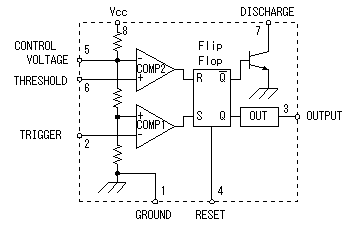
NE555 is composed of the voltage comparators, the flip-flop and the transistor for the discharge. The composition is simple, but it is excellent one.
Three resistors are connected with the inside in series and the power supply voltage(Vcc) is divided in 3. This composition is an excellent point. 1/3 with power supply voltage is applied to the positive input terminal of the comparator (COMP1) and the voltage of 2/3 is applied to the negative terminal of the comparator (COMP2). When the voltage of the trigger terminal(TRIGGER) is less than 1/3 of the power supply voltage, the S terminal of the flip-flop(FF) becomes H level and an FF is set. When the voltage of the threshold terminal(THRESHOLD) is more than 2/3 of the power supply voltage, the R terminal of the FF becomes H level and an FF is reset.


The oscillation operation explanation

    I will explain the circuit operation below.
The condition immediately after the turning on

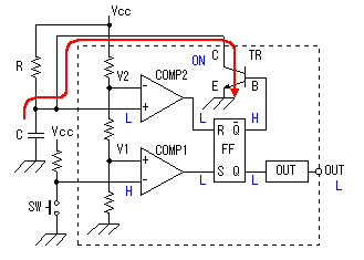
The condition when turning on the power becomes the condition which is shown in the figure on the left. The L is 0 V almost, showing the low level. H is the value which is high level and is near Vcc. The flip-flop (FF) is the SR type. The Q becomes H and becomes the L when S becomes H. After that, even if S becomes the L, the Q maintains H and maintains the condition of the L. When R becomes H, becomes H and the Q becomes the L. That is, the Q becomes H when a few S become H(the set) and the Q becomes the L when a few R become H(the reset). When S and R become H at the same time, the condition of the Q and is unsettled. (I think that both become H). Because is H in this condition, TR is in the ON condition and the collector (C) of TR is in the L condition. Therefore, the electric charge doesn't store up in capacitor(C), the (+) terminal with the voltage comparator(COMP2) doesn't cross V2. Because it is, the output of COMP2 is as the L and the FF doesn't become the reset condition. OUT is as the L condition.


The timer start condition

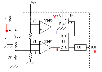
When the start switch (SW) is pushed, the COMP1 (-) terminal becomes the L condition.
Because the voltage of the COMP1 (-) terminal became equal to or less than V1 of the (+) terminal, the output of COMP1 becomes the H condition.
With this, the FF becomes the set condition, the Q changes into H, changes into the L condition and OUT becomes the H condition.
Because became the L condition, TR becomes the OFF condition. When TR becomes the OFF condition, the electric charge begins to store up in capacitor(C) through the resistor (R). As the electric charge stores up in capacitor(C), voltage of the both edges of capacitor(C) begins to go up. The start switch (SW) uses the non lock type which turns back after pushing once. In case of being as the pushed condition, OUT doesn't become the L condition even if the timer does in the time-out. When the start switch (SW) turns back, the COMP1 (-) terminal becomes the H condition and to become equal to or more than V1 of the (+) terminal, the output of COMP1 becomes the L condition. The output of COMP1 becomes the L condition and the S terminal of the FF becomes the L condition, the condition of Q and of the FF don't change. While the voltage of capacitor(C) doesn't exceed the voltage V2(the voltage of the COMP2 (-) terminal), FF maintains this condition.


The time-out condition

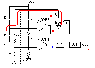
The output of COMP2 becomes the H condition when the electric charge stores up in capacitor(C) and the voltage of the COMP2 (+) terminal crosses V2 of the (-) terminal. The reset terminal (R) of the FF becomes the H condition with this, the Q becomes the L and becomes the H condition. OUT becomes the L condition.
Because becomes the H condition, TR becomes the ON condition. Because TR becomes the ON condition, the COMP2 (+) terminal becomes the L condition and the output of COMP2 returns to the L condition. So, the condition of the Q and don't change, OUT is as the L condition. Also, because TR becomes the ON condition, discharge through TR by the electric charge of capacitor(C) and the electric charge of capacitor(C) passes away.


By above operation, it returned to the condition before pushing the start switch.

Circuit and pattern drawings

|0 comments
555 timer
Circuit drawing


Pattern drawing
(Wiring side)

Tuesday, December 9, 2008

Time Delay Circuit

|0 comments

Time Delay Circuit

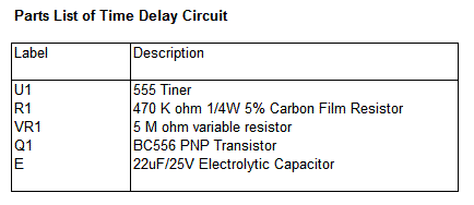
In the design of analog circuits, there are times when you would need to delay a pulse that came into a circuit before being used for the next process. This time delay circuit uses a 555 timer to delay a pulse that comes in to a maximum time of 75 seconds. The timing of the delay can also be changed by changing the resistor value of VR1 and the capacitor value of E based on the time delay formula of t=0.69RC.

In order for the output to go high, the reset pin of 555 timer (pin 4) must be high and the TRIGGER pin (pin 2) voltage level must be below a third of the level of the power supply to the IC. When there is no pulse being applied to the input, transistor Q1 will turn ON and capacitor E is charged.


Once a pulse is applied to the input, transistor Q1 will turn OFF and pin 4 reset pin is held to high. This caused the capacitor E1 to be discharged through VR1 resistor. The time delay will depend on the discharged of capacitor E to a third of the supply before the output of 555 goes high. Experiment with different values of VR1 and E to get different time delay.

If the maximum value of potentiometer is set to 5M ohm, the time delay of the pulse will be 75 seconds.


Parts List

Analog Timing Light Project

|0 comments
Timing Light Project

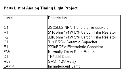
This analog timing light project uses RC circuit as a delay OFF timer to control the duration an incandescent light turns ON. When the accuracy of a timer is not critical, the use of RC circuit is a good choice as it is more cost effective and simple. Once the normally open switch SW is pressed, the light will turn ON for a duration of 10 - 20 seconds before it turns OFF. The duration of the turn ON time can be varied by varying the values of R1, R2 and E1.

Schematic Diagram

The schematic of the project is as shown below.

When SW is pressed, the base of the transistor Q1 is forward bias and it turns ON. This turns ON the 12V relay that is connected to the transistor. The contact of the relay RLY must be able to withstand the current of the load. At the same time, the electrolytic capacitor E1 is being charged to a voltage of approximately 0.7V.

Once SW is released, E1 will discharged through resistor R2 and the base of the transistor. After some time, When the voltage across E1 drops to approximately 0.5V, the transistor will turn OFF. This in turn will cause the relay to turn OFF and the incandescent light will turn OFF. The timing of the turn OFF can be changed by changing the values of E1, R1 and R2.

Parts List

The parts list of the project is as shown below.

Electronic Timer Switch

|0 comments

Electronic Timer Switch

This electronic timer switch project is a good project to build to simulate the presence of occupants in a house. In these days when security is becoming more of a concern when no one is at home, having this device will deter the thief from breaking in. When power up, after 60 minutes, the relay will turn ON for 100 secs, OFF for the next 100 secs, and ON again for 100 secs before OFF again for the next 60 mins. This sequence will be repeated. A device such as a lamp that is connected to the relay will turn ON and OFF according to this timing.


Schematic Diagram

The schematic of the project is as shown below.


The core of this electronic timer switch project uses a CD4060B binary counter. The binary counter has 10 outputs and the counter are counted by configuring the oscillator. Every negative clock will trigger the counter of the IC

internally.

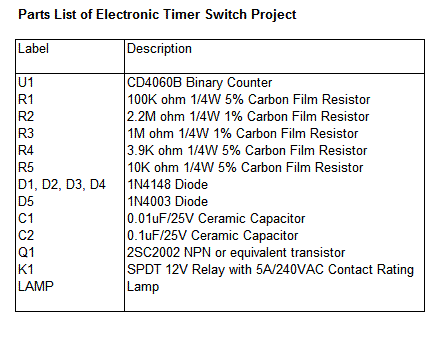
The timing of the circuit is affected by resistor R3(1M ohm) and capacitor C2(0.1uF). By connecting the four outputs in an AND configuration, the transistor Q1 will only turn ON if all the 4 outputs are in logic "1". If any of the logic is "0", the transistor will remain OFF.

For a complete cycle, the transistor will be ON twice when the output at pin 15, QJ goes to logic "1" and "0" twice when the other outputs QL, QM and QN remain at "1". When this happen, the relay K1 will switch status accordingly. The timing of the switching can be changed by changing the resistor values R2, R3 and C2. Download the data sheet of CD4060B from Texas Instrument website for more details.

Note that since the oscillator is not using crystal, the timing may not be as accurate compared to the ideal calculation. In most cases, fine tuning the resistor and capacitor are good enough to make this project a success. To check whether the circuit is working, connect a LED in series with a 390 ohm resistor at output QD. It will flash ON and OFF as the oscillator oscillates.


Parts List
555 Timer Program for Windows

|0 comments
** Works with Vista **
This program allows you to calculate Resistor and Capacitor values
for both Astable and Monostable modes.


Screenshot

555 Timer Program for Windows

555 Timer is fully working and free of charge.


Download 555 Timer

Download one of the archives,
then extract and run "555 Timer setup.exe"

555-Timer.zip

987KB

555-Timer.rar

895KB

Pluse Timer

|0 comments

Pluse Timer


R1 = 1 Meg, Preset Pot
R2 = 10K
R3,R4 = 1K
C1 = 10uF, 16V
C2 = 0.01uF
T1 = BC547 (Gen Purp NPN)
T2 = 2N2222 (Hi Current NPN)
D1 = 1N4001 (Gen Purp Si)
IC1 = 555 (Lo-Power version)
RLA1 = Relay, 9V (amps of your choice)


555 Timer Circuit

Power Supply

Electronic Circuit Designer.